Semiconductor packaging is one of the most thermally demanding applications in the entire molding industry. Unlike conventional injection molding where temperature uniformity of ±5–10°C is acceptable, semiconductor encapsulation molds require surface temperature uniformity of ±1–2°C across every cavity in a multi-cavity layout that may contain 64, 128, or even 256 individual package sites. At these tolerances, conventional drilled cooling lines are fundamentally inadequate.
This guide covers the specific thermal challenges of semiconductor packaging molds, explains why conformal cooling channels are uniquely suited to solve them, and provides the design parameters, material specifications, and performance data that semiconductor packaging engineers need to evaluate conformal cooling for their mold tooling. Whether you are encapsulating BGA, QFN, SiP, or lead frame packages, the thermal physics and the solutions are consistent.
1. Why Semiconductor Molds Demand Extreme Thermal Precision
Semiconductor encapsulation is not standard injection molding. The process uses epoxy molding compound (EMC) — a thermoset material that undergoes irreversible crosslinking during the molding cycle. Unlike thermoplastics that simply cool and solidify, EMC must reach a specific degree of cure (typically 85–95% conversion) within the mold before the package can be ejected. The cure reaction is exothermic and highly temperature-sensitive, making thermal control the single most critical process variable.
The consequences of thermal non-uniformity in semiconductor molds are severe and measurable:
- Wire bond sweep: Temperature gradients create differential EMC flow velocities across the cavity. In cavities that are too hot, the lower EMC viscosity causes higher flow velocity that physically displaces gold or copper wire bonds — a defect called wire sweep. Wire sweep rates above 3% typically trigger production line shutdown.
- Incomplete cure: Cavities running 5–8°C below target temperature exhibit 10–20% lower cure completion at the end of the molding cycle. Under-cured packages fail in downstream reliability testing (HTSL, TCT, HAST), generating costly field-return risk.
- Void formation: Non-uniform temperature creates non-uniform EMC gelation timing across the mold. Areas that gel prematurely trap volatiles, forming internal voids that degrade thermal and electrical performance of the finished IC package.
- Package warpage: Temperature-driven cure gradients across the top and bottom mold halves cause asymmetric CTE (coefficient of thermal expansion) buildup, warping the finished package. For BGA packages with solder ball pitch below 0.5 mm, warpage tolerance is typically <100 micrometers — achievable only with ±1–2°C mold temperature uniformity.
In semiconductor packaging, a 5°C mold temperature variation can cause a 15–20% difference in EMC cure completion across a multi-cavity mold. This is the root cause of the majority of encapsulation-related reliability failures. Conformal cooling eliminates this variation.
2. EMC (Epoxy Molding Compound) Behavior and Thermal Sensitivity
Understanding why semiconductor molds are so thermally sensitive requires understanding EMC material behavior. Epoxy molding compounds are fundamentally different from the thermoplastic resins used in conventional injection molding, and their thermal response dictates the cooling system requirements.
EMC Cure Kinetics: Why Temperature Matters
EMC cure follows an autocatalytic reaction model where the reaction rate is exponentially dependent on temperature. The practical implication is straightforward: a 5°C change in mold surface temperature changes the EMC cure rate by approximately 25–40%. This means that in a 128-cavity mold with ±8°C temperature variation (typical of conventional cooling), the fastest-curing cavities reach 95% cure while the slowest are still at 70–75% — far below the minimum 85% threshold for ejection.
| EMC Property | Value / Range | Cooling System Implication |
|---|---|---|
| Mold temperature range | 165–185 °C | Heating + cooling system must maintain elevated temperature with precision |
| Gel time at 175 °C | 8–15 seconds | Non-uniform temperature causes staggered gelation across cavities |
| Cure time at 175 °C | 60–120 seconds | Cycle time directly linked to slowest-curing cavity |
| Exothermic peak | 15–35 J/g | Cure reaction generates heat that must be managed to prevent thermal runaway |
| Thermal conductivity (cured) | 0.7–1.2 W/m·K | Low conductivity means heat extraction through mold steel is rate-limiting |
| Filler content (silica) | 70–90 wt% | High filler is abrasive — mold surface wear affects thermal contact over time |
| CTE (below Tg) | 8–15 ppm/°C | Mismatch with silicon die (2.6 ppm/°C) drives warpage if cure is non-uniform |
The Exothermic Challenge
Unlike thermoplastic molding where cooling simply removes the heat brought in by the melt, EMC encapsulation must manage the additional exothermic heat generated by the crosslinking reaction. In a 128-cavity mold with 3 mm average package thickness, the total exothermic heat load can reach 500–800 W during peak cure. If the cooling system cannot extract this heat uniformly, center cavities overshoot their target temperature by 5–10°C while edge cavities remain at setpoint — creating exactly the kind of thermal gradient that causes wire sweep and cure non-uniformity.
Conformal cooling channels positioned at uniform distance from every cavity surface ensure that the exothermic heat is extracted at the same rate from every package site. This is physically impossible with conventional straight-drilled cooling lines, which by geometric necessity are closer to some cavities than others.
3. Transfer Mold vs Compression Mold — Cooling Challenges Compared
Semiconductor packages are encapsulated using two primary molding processes: transfer molding and compression molding. Each process presents distinct thermal management challenges that conformal cooling addresses differently.
Transfer Molding
Transfer molding is the dominant encapsulation process for conventional IC packages (QFP, QFN, SOP, BGA). EMC is loaded as a pellet into a transfer pot, heated to reduce viscosity, and then plunger-driven through runners and gates into the mold cavities. The cooling challenges specific to transfer molding include:
- Runner-to-cavity temperature gradient: EMC flowing through the runner system picks up heat from the mold steel. Cavities nearest the runner are filled with hotter EMC than cavities at the end of the runner, creating a fill-temperature gradient of 3–8°C that adds to any mold surface temperature non-uniformity.
- Multi-plunger systems: Modern multi-plunger transfer molds (MPM) use 4–12 individual plungers to reduce flow length. Each plunger zone must be thermally independent. Conventional cooling cannot provide per-zone thermal control without extremely complex manifolding.
- Cull plate thermal management: The cull — the disc of cured EMC remaining in the transfer pot — must reach a specific cure level before ejection. The cull plate area requires independent cooling that does not interfere with cavity cooling.
Compression Molding
Compression molding is used for advanced packages including fan-out wafer-level packages (FOWLP), panel-level packages, and large-area encapsulation. EMC (often in granular or liquid form) is placed directly on the substrate, and the mold closes to compress the material into shape. Compression molding cooling challenges include:
- Large-area uniformity: Compression molds for panel-level packaging can exceed 600 mm × 600 mm. Maintaining ±1°C across this area with conventional cooling requires an impractical number of drilled lines and creates excessive pressure drop.
- Thin package profiles: Compression-molded packages may be as thin as 0.15–0.30 mm. At this thickness, the EMC thermal mass is extremely low, and the package temperature is essentially determined by the mold surface temperature. Any mold temperature non-uniformity maps directly to package defects.
- Vacuum channel integration: Compression molds require vacuum channels to remove trapped air before compression. These channels occupy space in the mold steel that would otherwise be available for cooling lines, making geometric conflicts between vacuum and cooling systems a persistent design challenge.
| Parameter | Transfer Mold (Conventional) | Transfer Mold (Conformal) | Compression Mold (Conformal) |
|---|---|---|---|
| Mold surface ΔT | ±5–12 °C | ±1–2 °C | ±0.8–1.5 °C |
| Cavity-to-cavity variation (128-cavity) | 8–15 °C range | 2–3 °C range | N/A (single cavity) |
| Typical cycle time | 90–150 seconds | 65–110 seconds | 45–80 seconds |
| Wire sweep defect rate | 1.5–4.0% | 0.2–0.8% | N/A (typically no wire bonds) |
| Package warpage control | ±80–200 μm | ±30–60 μm | ±20–50 μm |
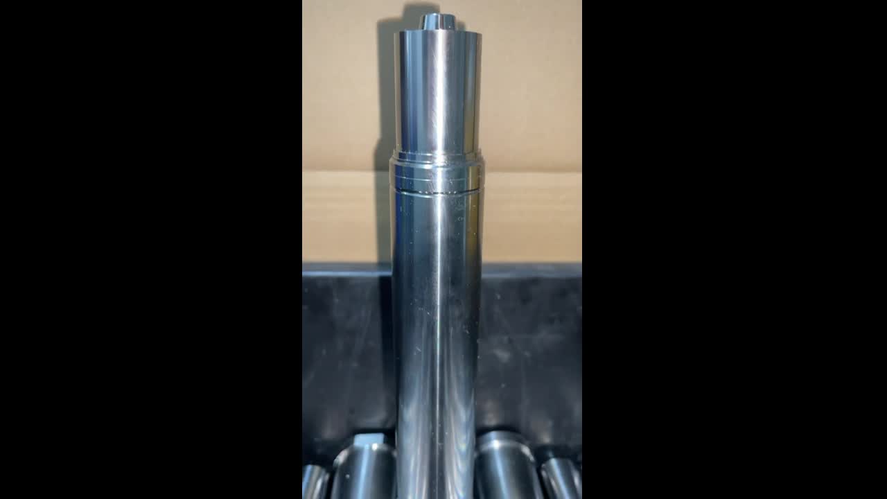
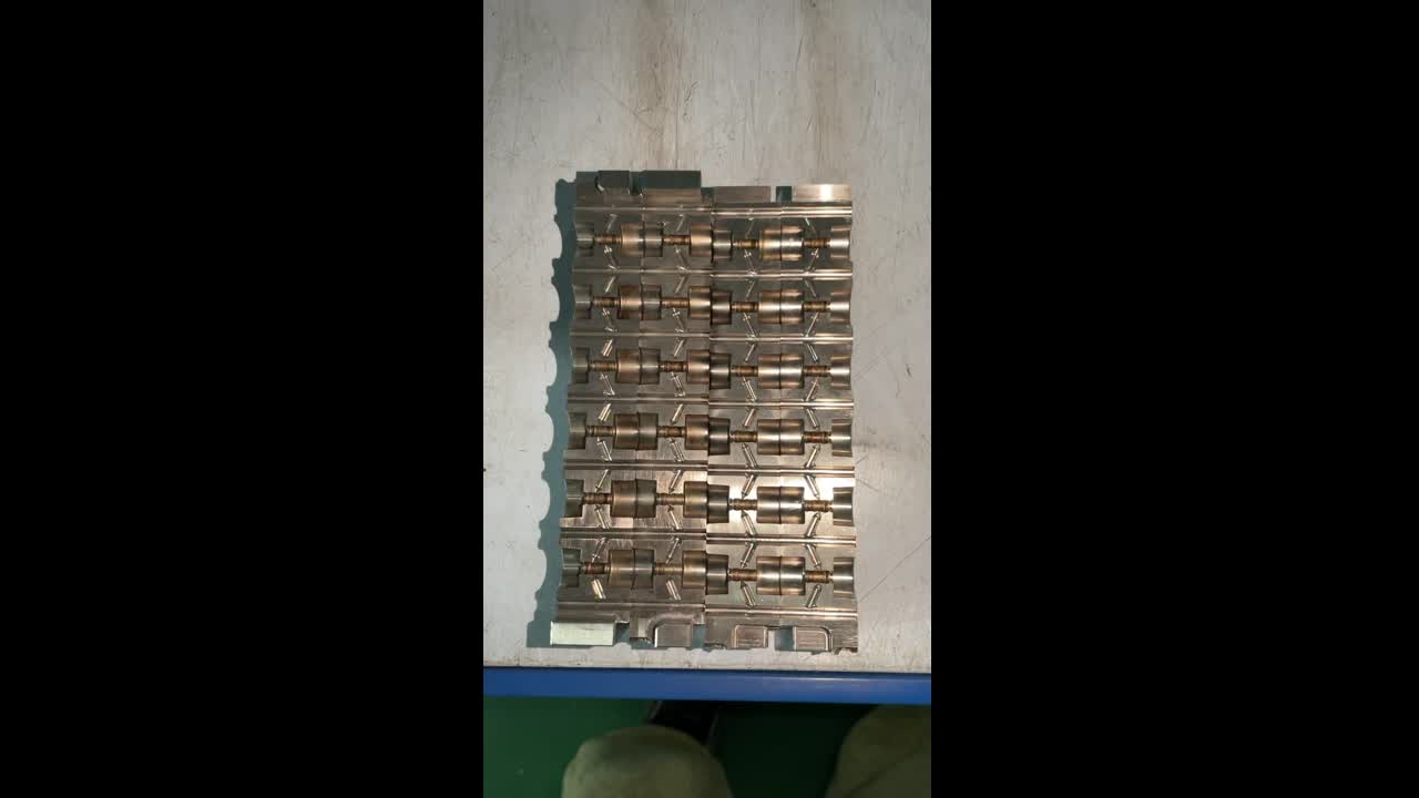
4. Thin-Wall Lead Frame Cooling — The Sub-Millimeter Challenge
Lead frame packages (QFP, QFN, SOP, SOT) present the most geometrically constrained cooling challenge in semiconductor packaging. The mold cavities for these packages are shallow (0.4–1.2 mm EMC thickness above the die) and densely packed (0.8–2.5 mm pitch between adjacent cavities). The lead frame itself — a thin copper alloy strip 0.15–0.25 mm thick — sits between the top and bottom mold halves, dividing the cavity into two ultra-thin sections that must be cooled from both sides simultaneously.
Why Conventional Cooling Fails on Lead Frame Molds
The fundamental problem is geometric: a drilled cooling line has a minimum practical diameter of 4–6 mm (to allow adequate flow rate and prevent fouling), and it must be positioned at least 5–8 mm from the mold surface to maintain structural integrity of the steel above it. In a lead frame mold where the cavity depth is only 0.8 mm, a cooling line at 6 mm depth is cooling through 7.5 times the thickness of the molded part. The thermal resistance of this steel thickness creates a thermal lag that makes precise temperature control impossible.
Channel-to-surface distance: Reduced from 6–8 mm (drilled) to 2.5–3.5 mm (conformal) — a 55–60% reduction in thermal resistance.
Channel geometry: Elliptical cross-section (1.8 mm × 3.0 mm) instead of circular (5 mm diameter) — fits between closely spaced cavities without structural compromise.
Surface temperature response time: Reduced from 8–12 seconds (drilled) to 2–4 seconds (conformal) — enabling real-time thermal control that tracks the EMC exothermic reaction.
Temperature uniformity across 256 QFN sites: Improved from ±8°C to ±1.5°C — bringing all cavities within the acceptable cure window simultaneously.
The ability to use small-diameter, non-circular channel cross-sections is a unique advantage of 3D-printed conformal cooling. Conventional machining is limited to circular cross-sections in straight lines. SLM printing can produce elliptical, teardrop, or rectangular channels that follow the cavity layout at pitches as tight as 3–4 mm — matching the cavity pitch of modern high-density lead frame molds.
5. BGA, QFN, and SiP Package Mold Examples
The following examples illustrate conformal cooling performance across three common semiconductor package types, each with distinct thermal management requirements.
Challenge: The 128-cavity layout created a center-to-edge temperature gradient of 12°C with conventional cooling. Center cavities exhibited 3.2% wire sweep rate and 150–200 μm package warpage, exceeding the <100 μm specification for board-level reliability.
Conformal cooling solution: Spiral conformal channels (2.5 mm diameter) positioned 3.0 mm from cavity surface, with independent circuits for center zone, intermediate zone, and edge zone. Flow rate balanced to compensate for center-zone exothermic heat concentration.
Results:
- Temperature uniformity: ±10°C → ±1.5°C
- Cycle time: 120 seconds → 88 seconds (27% reduction)
- Wire sweep rate: 3.2% → 0.4%
- Package warpage: 175 μm → 55 μm (within specification)
Challenge: Ultra-thin package height (0.85 mm) with only 0.4 mm EMC above the die. Conventional cooling at 7 mm depth could not respond fast enough to track the exothermic peak, causing 5–8°C overshoot in center sites. Void rate exceeded 2% on inner sites due to premature gelation at higher temperature.
Conformal cooling solution: Elliptical channels (1.5 mm × 2.8 mm) at 2.8 mm from surface, following a serpentine path that weaves between the 256 cavity positions. Channel pitch matched to cavity pitch at 3.8 mm. Independent top and bottom mold circuits with differential flow rates to balance CTE-driven warpage.
Results:
- Temperature uniformity: ±7°C → ±1.2°C
- Cycle time: 95 seconds → 68 seconds (28% reduction)
- Void defect rate: 2.3% → 0.3%
- Incomplete cure rejects: 1.8% → 0.1%
Challenge: SiP packages contain 2–4 stacked dies with multiple wire bond tiers. The tall wire loops (up to 175 μm) require very low EMC flow velocity during compression, which means long fill times and extended thermal exposure. The multi-die stack creates localized thermal mass variation — areas above 4-die stacks retain more heat than areas above 2-die stacks, creating intra-cavity temperature gradients of 4–6°C.
Conformal cooling solution: Variable-density conformal channels with tighter channel spacing (3.5 mm pitch) above 4-die stack zones and wider spacing (5.0 mm pitch) above 2-die zones, creating a thermal impedance map that compensates for the die-stack thermal mass variation. Channel cross-section: 2.0 mm diameter circular.
Results:
- Intra-cavity temperature uniformity: ±5°C → ±1.8°C
- Cycle time: 135 seconds → 98 seconds (27% reduction)
- Wire sweep on Tier 3/4 bonds: 4.5% → 0.6%
- Package coplanarity: 85 μm → 35 μm
6. Conformal Cooling Design Parameters for Semiconductor Molds
Designing conformal cooling for semiconductor molds requires tighter dimensional control than standard conformal cooling design for injection molding. The following parameters have been validated across multiple semiconductor packaging mold programs.
| Design Parameter | Standard Injection Mold | Semiconductor Packaging Mold | Rationale |
|---|---|---|---|
| Channel-to-surface distance | 8–15 mm | 2.5–4.0 mm | Minimizes thermal resistance for ultra-thin cavities |
| Channel diameter / cross-section | 4–8 mm circular | 1.5–3.0 mm elliptical or circular | Fits between closely-spaced cavity positions |
| Channel pitch | 2–3× diameter | 1.5–2.5× width | Higher density required for ±1–2°C uniformity |
| Target temperature uniformity | ±5–10 °C | ±1–2 °C | EMC cure kinetics demand tight thermal control |
| Coolant temperature | 20–80 °C (water) | 150–200 °C (oil) | Operating temperature above water boiling point requires thermal oil |
| Coolant flow rate | 5–15 L/min per circuit | 2–6 L/min per circuit | Smaller channels with higher fluid velocity for turbulent flow |
| Reynolds number target | >10,000 | >4,000 (oil at 170°C) | Oil viscosity at high temp allows turbulence at lower Re |
| Surface roughness (channel interior) | <15 μm Ra | <10 μm Ra | Smoother channels resist fouling from thermal oil degradation products |
| Pressure drop budget | 2–5 bar per circuit | 3–8 bar per circuit | Higher pressure drop acceptable for precision thermal control |
It is critical to verify these parameters using thermal simulation before committing to print. Semiconductor molds operate at elevated temperatures where thermal oil properties (viscosity, heat capacity) change significantly — a design validated at 175°C may underperform at 185°C if the flow regime transitions from turbulent to laminar due to oil viscosity changes.
7. Material Selection for Conformally Cooled Semiconductor Molds
Semiconductor packaging molds operate under conditions that are significantly more demanding than standard injection molds: higher temperatures (165–185°C continuous), corrosive EMC filler chemistry, and extreme surface finish requirements. Material selection must balance thermal conductivity, hardness, corrosion resistance, and printability.
| Property | Maraging Steel (MS1 / 1.2709) | CX Stainless Steel | H13 Tool Steel |
|---|---|---|---|
| Hardness (after heat treatment) | 50–54 HRC | 48–52 HRC | 46–50 HRC |
| Thermal conductivity | 20–25 W/m·K | 15–18 W/m·K | 24–28 W/m·K |
| Corrosion resistance | Moderate — requires surface coating for high-Cl EMC | Excellent — inherent stainless properties | Low — requires hard chrome plating |
| SLM printability | Excellent — well-characterized process | Good — proven on EOS/SLM Solutions platforms | Challenging — prone to cracking without preheat |
| Surface finish (post-machined) | <0.2 μm Ra achievable | <0.2 μm Ra achievable | <0.2 μm Ra achievable |
| Density (as-printed) | >99.5% | >99.5% | 99.0–99.5% |
| Best suited for | General semiconductor molds, standard EMC | High-chloride EMC, green compound molds | Low-volume prototype molds only |
Surface Coating Considerations
Semiconductor mold surfaces are typically coated with hard chrome (5–15 μm) or TiN/CrN PVD coatings (2–5 μm) to resist EMC adhesion and filler abrasion. These coatings are fully compatible with SLM-printed conformal cooling inserts — the insert is post-machined to final dimensions and then coated using the same process applied to conventionally manufactured mold components. The key requirement is that the conformal cooling channels must be sealed and leak-tested before coating, as coating processes (especially electroplating) can deposit material inside any exposed channel openings.
Thermal Oil Compatibility
At operating temperatures of 165–185°C, water-based cooling is not feasible. Semiconductor molds use thermal oil (typically synthetic heat transfer fluid rated to 300°C) as the cooling/heating medium. Conformal cooling channel design must account for oil properties that differ significantly from water:
- Lower thermal conductivity: Thermal oil at 175°C has a thermal conductivity of approximately 0.11 W/m·K versus 0.67 W/m·K for water at 60°C. This 6× lower conductivity means that turbulent flow is essential — laminar flow in oil provides grossly inadequate heat transfer.
- Higher viscosity range: Oil viscosity at 175°C is typically 0.8–1.5 cP, which is actually comparable to water at 60°C (0.47 cP). However, during startup when the oil is cold, viscosity can be 50–100 cP, creating a risk of laminar flow and uneven heating during the preheat phase.
- Fouling potential: Thermal oil degrades over time at elevated temperature, forming carbon deposits and sludge that can partially block small-diameter conformal channels. Channel interior surface roughness below 10 μm Ra and regular oil analysis (every 2,000 operating hours) are essential maintenance requirements.
8. FAQ — Conformal Cooling in Semiconductor Packaging
Semiconductor packaging molds require temperature uniformity of ±1–2°C across the entire mold surface to ensure consistent EMC cure, prevent wire bond sweep, and avoid incomplete fill in thin-section cavities. Conventional drilled cooling lines cannot achieve this level of uniformity on multi-cavity molds with 64 to 256 cavities. Conformal cooling channels follow the cavity contour at a uniform distance, delivering the thermal precision that semiconductor encapsulation demands.
Conformal cooling consistently achieves mold surface temperature uniformity of ±1 to 2 degrees C on semiconductor packaging molds, compared to ±5 to 12 degrees C with conventional drilled cooling. This improvement is critical because EMC cure kinetics are exponentially temperature-sensitive — a 5 degree C variation can cause 15 to 20 percent difference in cure completion across a multi-cavity mold, leading to package delamination, void formation, and wire bond reliability failures.
Yes. Conformal cooling typically reduces transfer mold cycle time by 20 to 30 percent on semiconductor packaging applications. The cycle time reduction comes from two mechanisms: faster and more uniform heat-up to the target mold temperature of 165 to 185 degrees C, and more uniform EMC cure across all cavities, allowing the cure time to be set by the average cavity performance rather than the slowest cavity. On a 128-cavity BGA mold running 3,000 or more shots per day, a 25 percent cycle reduction translates to 750 additional units per day.
For semiconductor packaging molds operating at 165 to 185 degrees C, maraging steel (1.2709 or MS1) printed via SLM is the preferred material. It offers 50 to 54 HRC hardness after aging, thermal conductivity of 20 to 25 W/m K, and acceptable resistance to standard EMC formulations. For molds requiring superior corrosion resistance due to high-chloride EMC chemistry, CX stainless steel at 48 to 52 HRC provides better chemical resistance with a modest thermal conductivity trade-off.
Semiconductor packaging molds run extremely high shot volumes — typically 500,000 to 5 million shots per year per mold. At these volumes, even a 20 percent cycle time reduction delivers payback within 1 to 5 days. The yield improvement from better temperature uniformity — reducing incomplete cure, wire sweep, and void defects by 40 to 70 percent — provides quality savings that often exceed the throughput savings. For a 128-cavity BGA mold, total annual savings from conformal cooling typically range from $150,000 to $400,000.
Related Pages
- Conformal Cooling Benefits — Five Benefit Categories with a 3-Year Factory Model
- Conformal Cooling Channel Design — Diameter, Pitch, and Depth Rules
- Conformal Cooling Materials — Maraging Steel, CX Stainless, and H13 Compared
- Conformal Cooling Simulation — Moldflow and Thermal FEA Workflow
- Conformal Cooling vs Conventional Cooling — Side-by-Side with 13 Real Projects
- Conformal Cooling Inserts — Service Details & Specifications
- Case Studies — Full Production Data from Real Programs